Guias Tecnicas
1 abr 202616 min
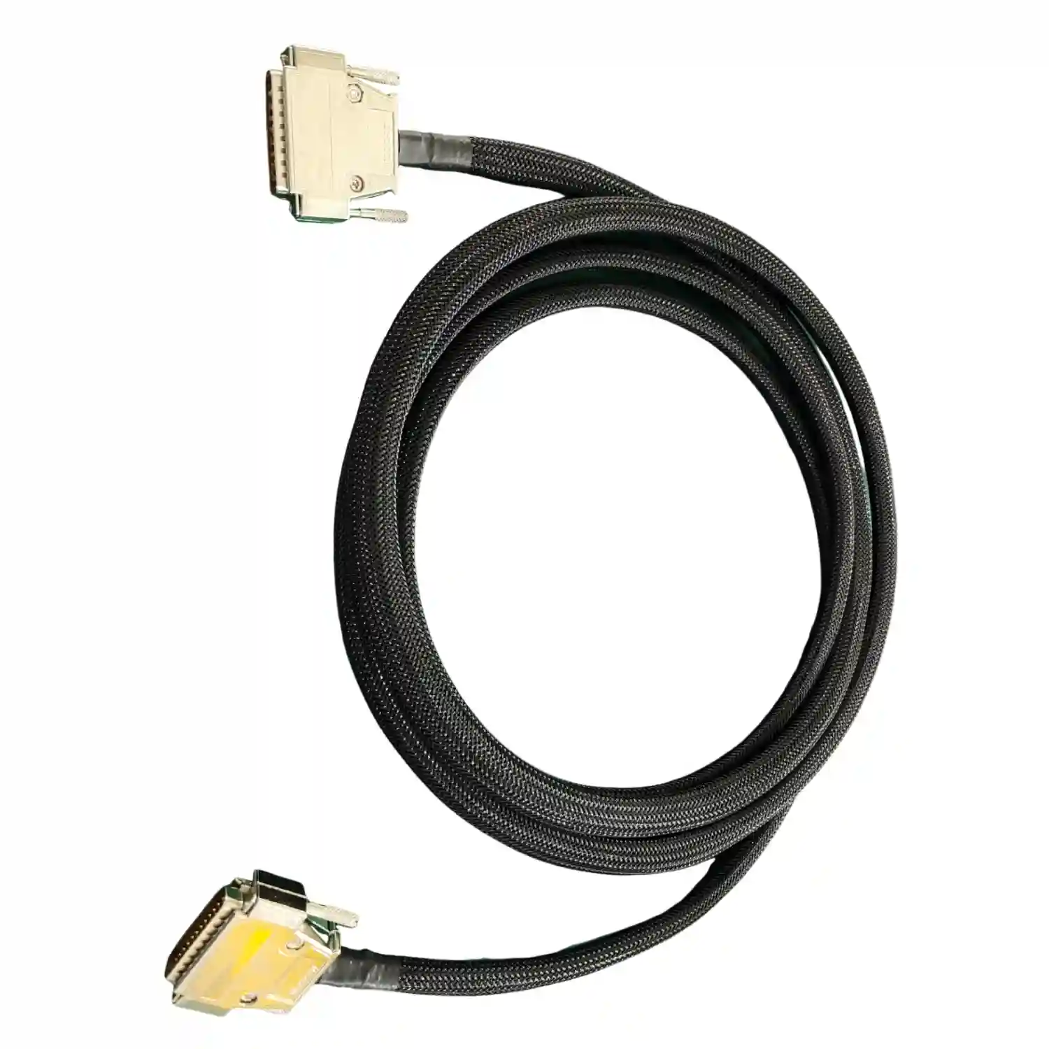
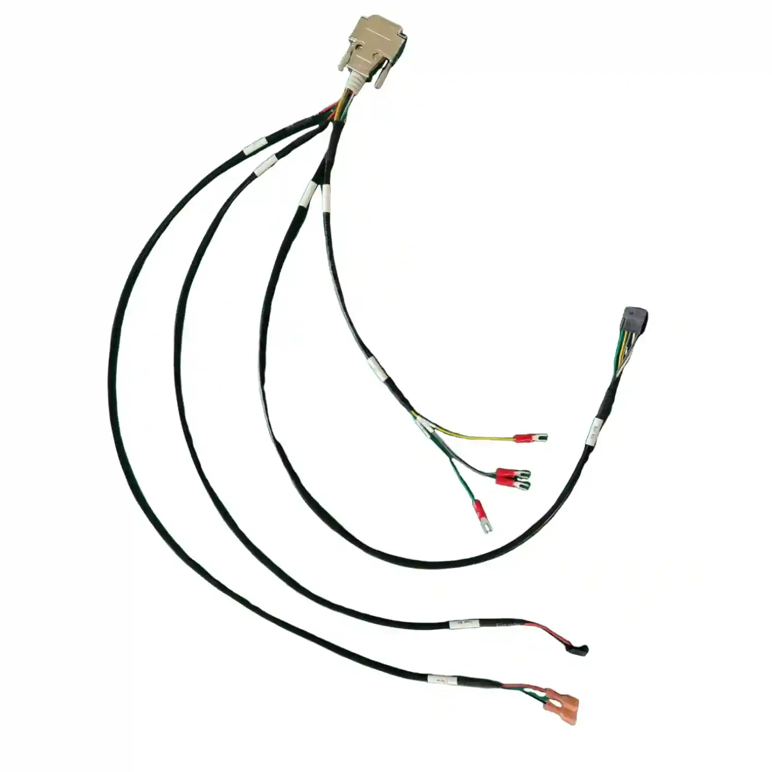
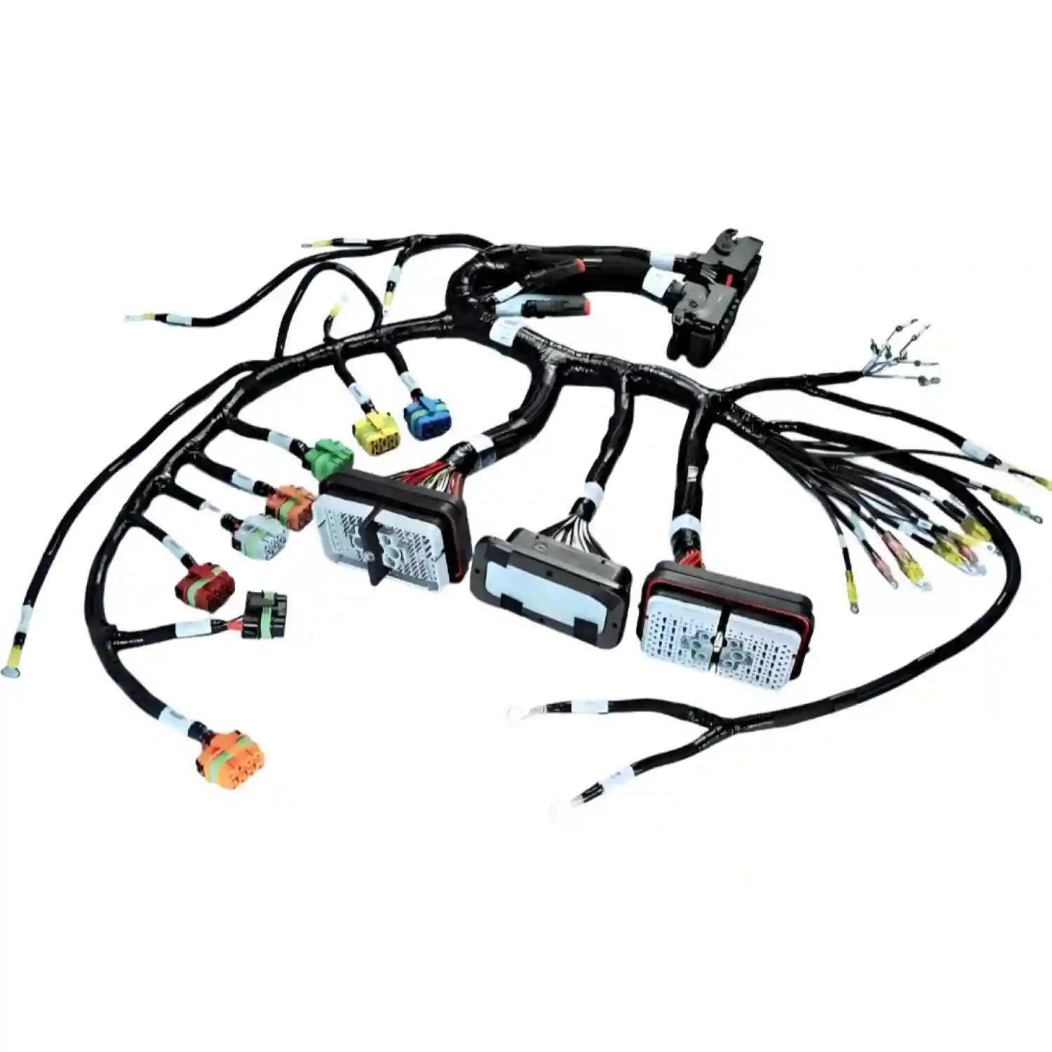
Materiales para Arneses de Cables: Guia Completa de Conductores, Aislantes y Conectores
Guia tecnica de materiales para arneses de cables: cobre vs aluminio, aislantes PVC vs XLPE vs silicona vs PTFE, terminales estañados vs niquelados, protecciones mecanicas, seleccion por industria (automotriz, medica, industrial) y normas SAE J1128, UL 758, IPC/WHMA-A-620.
Arneses de CablesMateriales ConductoresAislamiento Cables
LEER MÁS